SAN FRANCISCO – Jan. 30, 2025 – CEA-Leti scientists presented three papers at Photonics West 2025 detailing the institute’s latest R&D successes to improve chemical detection, high-speed communication and LIDAR performance with integrated optics on silicon.
“Integrated optics on silicon will play an increasingly vital role in many diverse and critical applications, because photonic integrated components are compact, easy to manufacture and they allow integration of advanced materials,”
said Cyril Fellous head of CEA-Leti's Optics and Photonics Division.
“Because all passive functions of the lasers, such as optical feedback, waveguide routing, and power transfer, are defined into the silicon, more degrees of freedom are allowed for the design,”
said Maxime Lepage, lead author of the paper. “Chemical sensing has become an active research area and a key application for mid-IR silicon-photonic devices due to their growing potential in spectroscopy, material processing, chemical and biomolecular sensing, security, and industrial applications,”
Lepage explained.
This innovative design improves the optics of frequency modulation continuous wave (FMCW) flash LiDAR by integrating critical components into a single device, opening opportunities for compact and efficient LiDAR systems for applications such as autonomous driving, facial recognition and robotics.
“This integrated version of the illumination optics of an FMCW flash LIDAR is a first step towards an integrated version of this type of LIDAR,”
explained the paper’s lead author, Paul Camus.
The paper, “
Towards Fully Integrated Frequency Comb Based Transceivers”, reports advances in nonlinear photonics for high-speed communications on a silicon-nitride platform. The team fabricated ultralow-loss SiN waveguides and components on a 200mm wafer to generate a frequency comb and separate the comb lines. Such a circuit would reduce cost and consumption of high-speed transmitters by replacing many lasers with a single frequency comb source.
Optical frequency combs are a type of optical signal that contains many discreet and very stable wavelengths spaced regularly, thus acting as multiple parallel laser sources. They are generated using nonlinear optical processes in suitable materials, such as SiN.
“This achievement is an important step towards a fully integrated photonic transmitter based on nonlinear photonics,”
said Baptiste Routier, lead author of the paper. “Those functions have been demonstrated separately, or if on the same chip, on different layers of materials. To our knowledge, it is the first time this has been achieved on the single layer, which is important because it simplifies the fabrication process and enhances overall device reliability.”
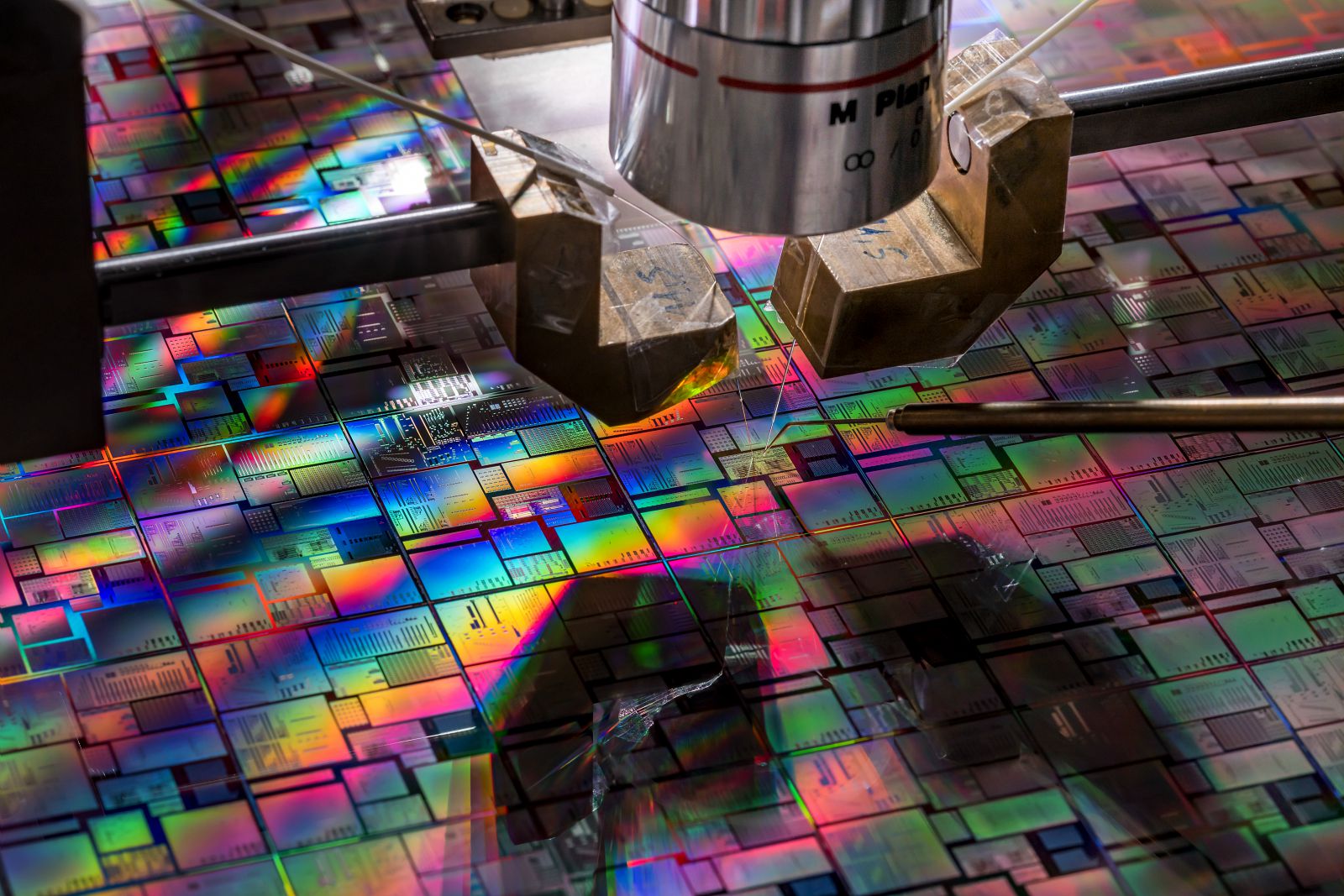 Automated wafer level electro-optical probe testing of silicon photonics.
About CEA-Leti (France)
CEA-Leti, a technology research institute at CEA, is a global leader in miniaturization technologies enabling smart, energy-efficient and secure solutions for industry. Founded in 1967, CEA-Leti pioneers micro-& nanotechnologies, tailoring differentiating applicative solutions for global companies, SMEs and startups. CEA-Leti tackles critical challenges in healthcare, energy and digital migration. From sensors to data processing and computing solutions, CEA-Leti's multidisciplinary teams deliver solid expertise, leveraging world-class pre-industrialization facilities. With a staff of more than 2,000 talents, a portfolio of 3,200 patents, 11,000 sq. meters of cleanroom space and a clear IP policy, the institute is based in Grenoble, France, and has offices in Silicon Valley, Brussels and Tokyo. CEA-Leti has launched 76 startups and is a member of the Carnot Institutes network. Follow us on
www.leti-cea.com and @CEA_Leti.
Technological expertise
CEA has a key role in transferring scientific knowledge and innovation from research to industry. This high-level technological research is carried out in particular in electronic and integrated systems, from microscale to nanoscale. It has a wide range of industrial applications in the fields of transport, health, safety and telecommunications, contributing to the creation of high-quality and competitive products.
For more information:
www.cea.fr/english